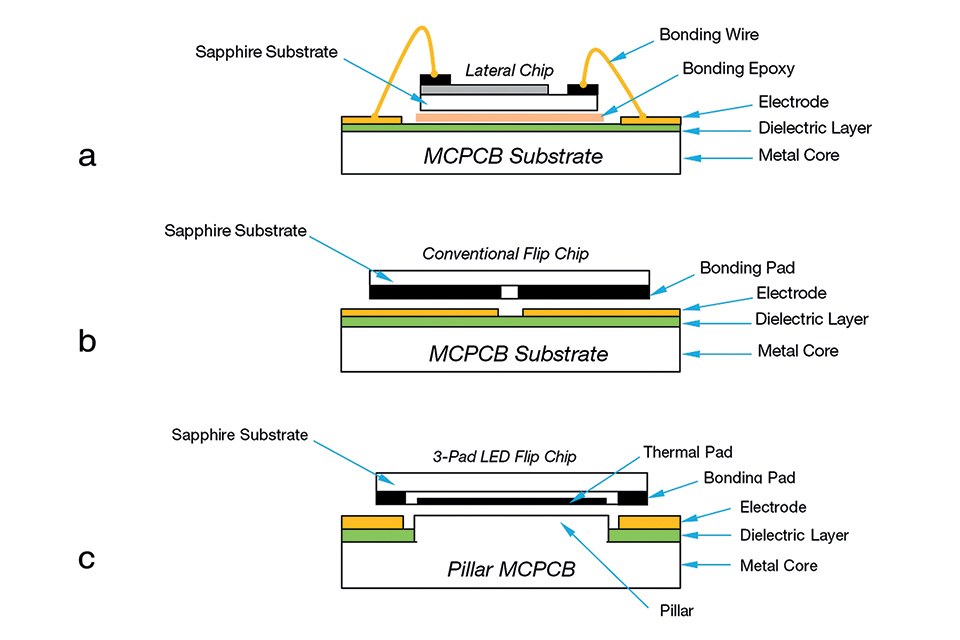
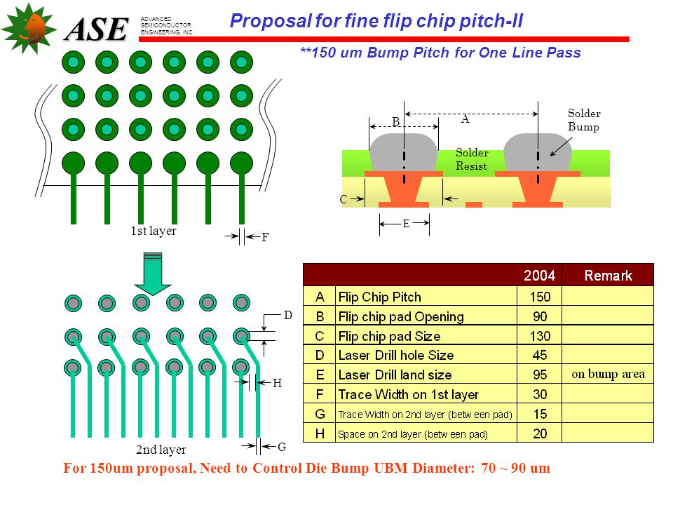
Details of test chip designs: pad pitch, layout, materials, and opening.
4.7 (401) · $ 20.50 · In stock

ASE Flip-Chip Build-up Substrate Design Rules - ppt video online download
Details of test chip designs: pad pitch, layout, materials, and opening.

Taking on the 0.3 mm ultra-fine pitch device challenge in PCB design
IC I/O pad layout and choice

Flip-Chip - Semiconductor Engineering

What is Pad to Pad (PP) ?

Details of test chip designs: pad pitch, layout, materials, and opening.
Pad Layout - Johanson Technology

AN-772: A Design and Manufacturing Guide for the Lead Frame Chip Scale Package (LFCSP)

Scaling Bump Pitches In Advanced Packaging

What is a Pad in PCB Design and Development
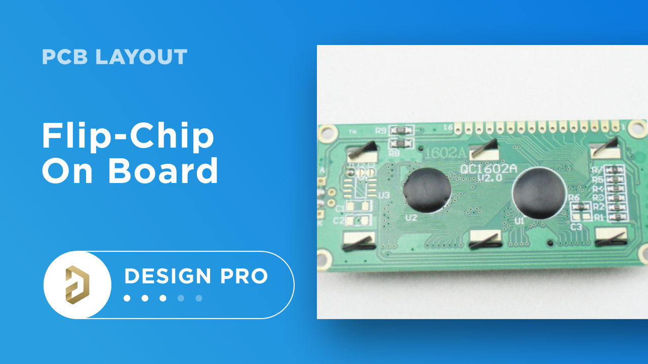
PCB Design Rules for Chip-on-Board Layout

Upper part: Layout of the flip-chip with 60 μm solder spheres applied